Analog Output
Introduction
The FPGA is a digital device. We convert the binary numbers (like 0, 1, 10, 11...) in the FPGA to voltages (like 0 mV, 1 mV, 2 mV...) using a digital to analog converter.
With the GoBoard and the Lattice UltraPlus boards I am using the Digilent Pmod DA3 which has a 16 bit serial interface,
With the DE0-nano board I am using a Linear Technology (now Analog Devices) board, the 2459A, which has a 16 bit parallel interface.
Because of the different interfaces, using the two DAC boards is very different.
Using the Digilent Pmod DA3 DAC
Since the Digilent board is a serial device sending data to it is very similar to the UART transmitter in the NandLand tutorials. Link to UART transmitter tutorial.
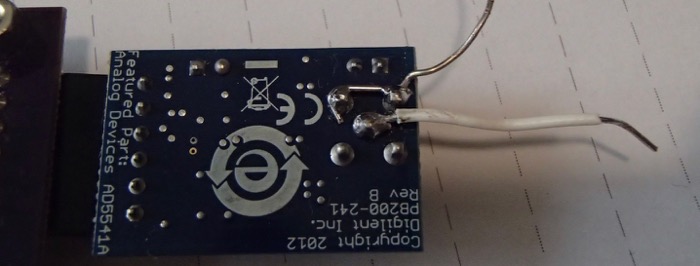
Designing the FPGA circuit requires information from the datasheet of the DAC circuit on the board, the Analog Devices AD5541A. The crucial information is represented by the timing diagram from the datasheet.
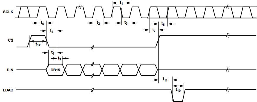
These are the signals we must send to the Digilent PmodDA3 board, which is only a simple carrier for the DAC chip. Refering to the timing diagram, we have:
SCLK goes through Pmod connector pin 4. Frequency can be as high as 50 MHz, so we send the GoBoard's 25 MHz clock, inverted. (Why inverted? See below.)
~CS goes through Pmod connector pin 1. "CS" means "chip select" and the "~" and "bar" both mean inverted logic where true means false and false means true. We could say that thsi line is "active low." The point is that the AD5541 chip will ignore data signals until CS goes low. It will then accept 16 data bits. After that, CS should go high and the DAC will then set the analog output voltage ased on the data.
DIN goes through Pmod connector pin 2. "DIN" means "data in." It must be set high or low 16 times to represent 16 "1" or "0" bits. Notice t8 and t9 in the diagram. They are telling us that the data bits must be set to "1" or "0" and not change during the rising edge of the clock. This is crucial but easy to arrange. In the FPGA projects we are doing in the tutorials, all the changes happen on rising clock edges. So to satisfy the DAC's need for stable data bits on the rising clock edge we delay the clock by 1/2 cycle, which is done by inverting the clock.
~LDAC goes through Pmod connector pin 3. "LDAC" means "Load DAC" (educated guess) and the "~" or "bar" means that it is "active low." When LDAC goes low, the data that has arrived is loaded into the analog output. In this application, we're holding it low always, so the analog output happens as soon as the last serial data bit is received. We could potentially use LDAC to synchronise the analog output to some other signal.
The examples on the next two pages do these things. Download and try them!
Testing DAC functionality
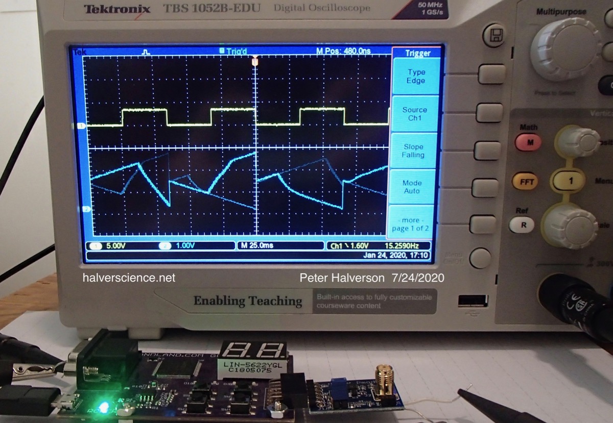
Build and load the code on the next page (Analog Out, Verilog 1), choosing the "Make_Test_Waveform_Sawtooth."
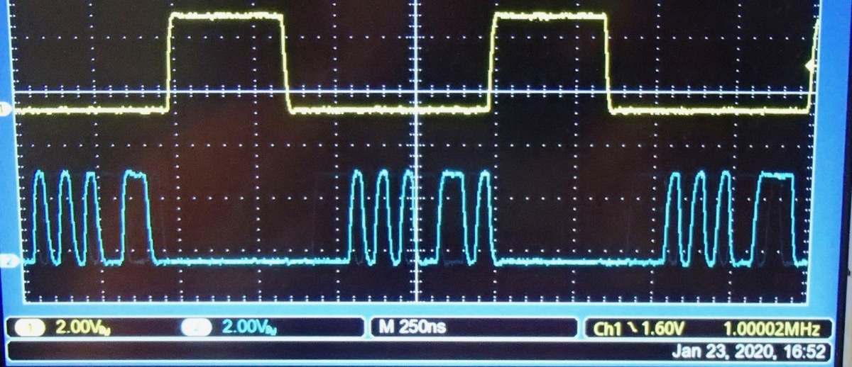
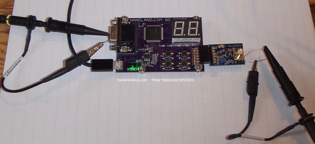
If you are using the GoBoard, a convenient way to trigger your oscilloscope is to connect to the currently unused VGA_VSync line as shown here:
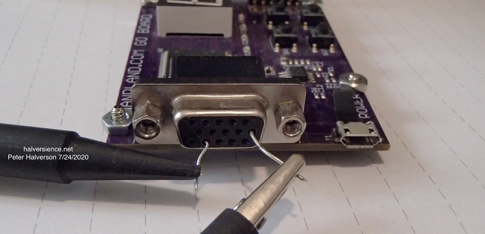
You also need to connect the scope to the DA3 output. The SMA connector was inconvenient for me, so here is what I did...
(I later learned that Digilent sells SMA to alligator clip connectors. Link to SMA-alligator connector. )
So the setup looks like this:
When you load the sawtooth version of DAC_Test_Top.v here is what you should see:
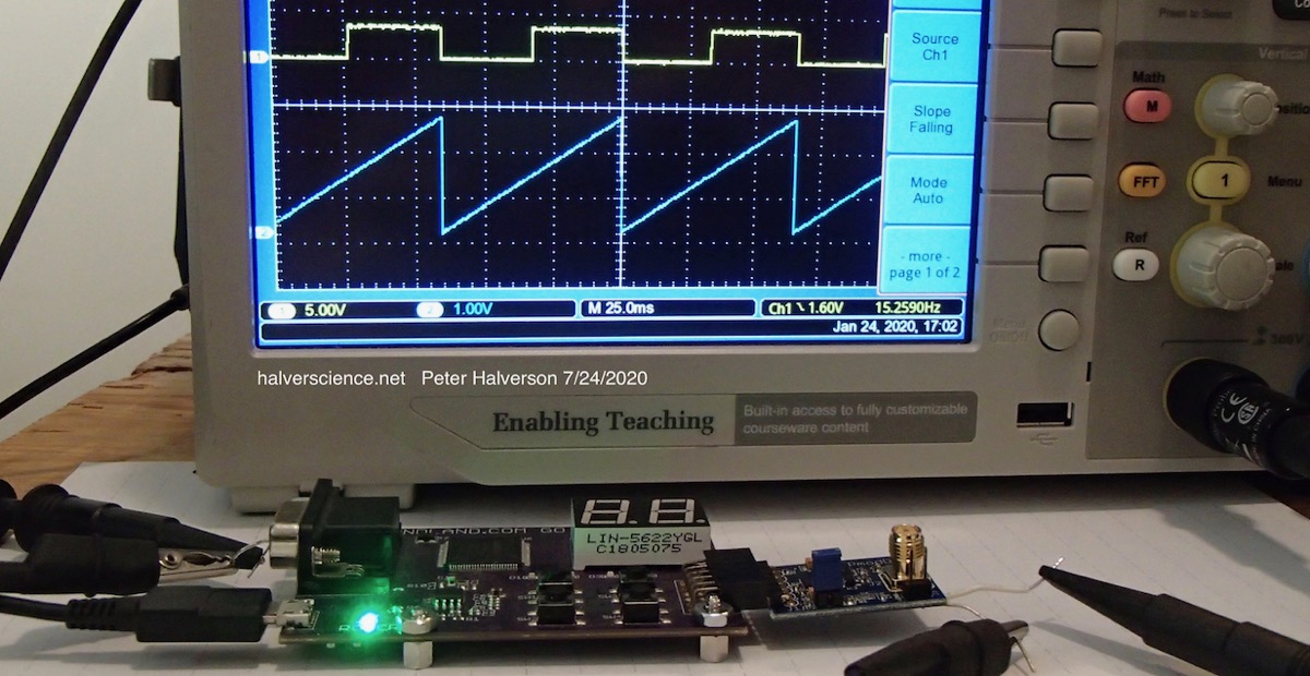
(Note that the Pmod DA3 is plugged into the lower row of the GoBoard's Pmod connector.)
Testing DAC Performance
The sawtooth pattern in the picture above tells us that the DAC is functional. However, this is the easiest possible task for a DAC. We need a test that exercises its dynamic capabilities: high slew rate, short settling settling time. My experience is that DAC sometimes fail to meet expectation.
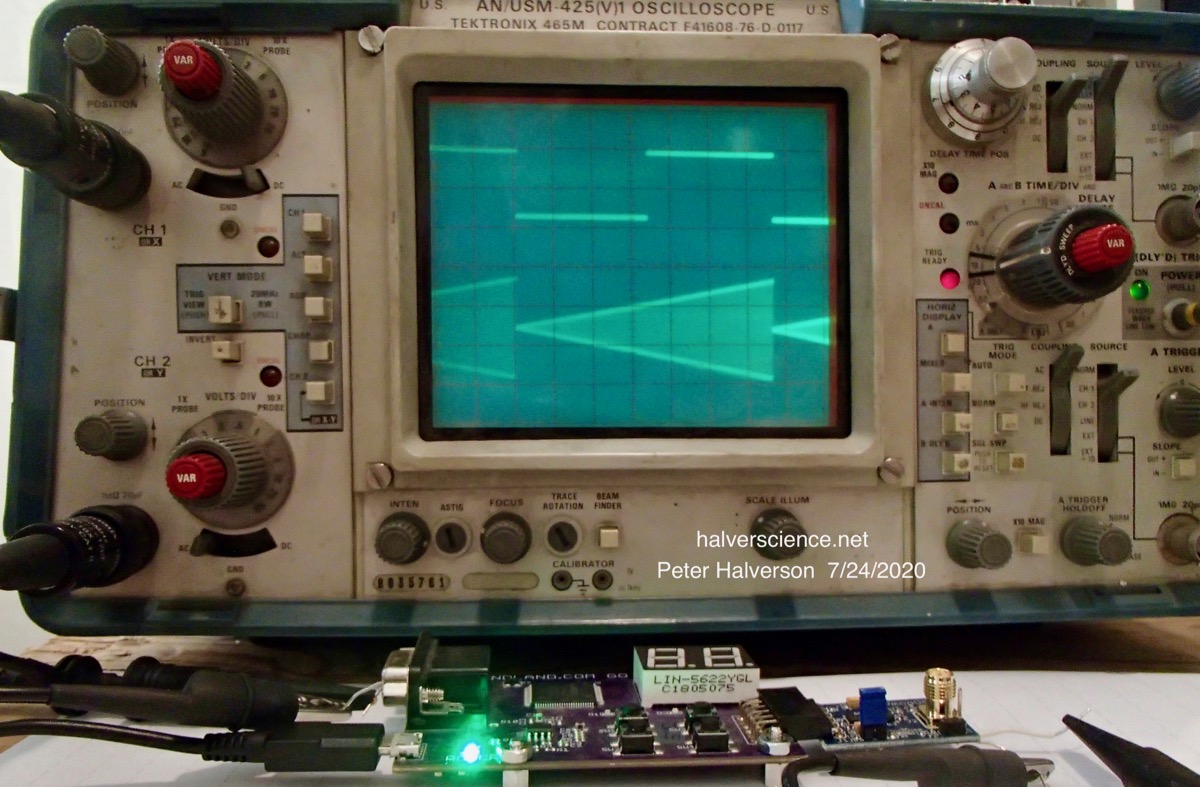
The second test on the next page, the "Growing_Squarewave" does the job. The DAC has to generate a 500 kHz squarewave whose amplitude grows linearly. I.e., sawtooth amplitude modulation. Its exercises all the DAC codes and requires maximum slew rate. This test revealed subtle bugs in my Verilog, ut the DAC passes the test. (On the other hand, the Digilent DA2 DAC board has trouble with this test.)
Unfortunately, this test is beyond the capabilies of most digital oscilloscopes, so to see the outcome, you will need a fast analog scope. My analog scope sees a smoothly increasing amplitude square wave (good!) and my digital scope sees nonsense (not due to the DAC).
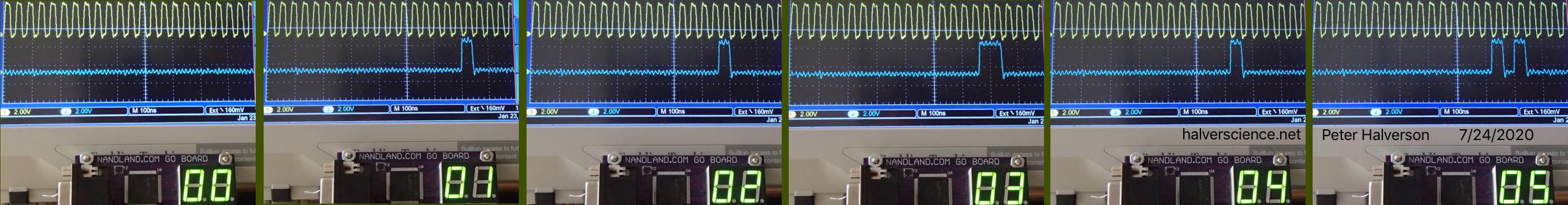
If you don't have an analog scope handy, use the code on the "Analog Out, Verilog 2" page. It sets up four test modes that you can select using the pushbutton switchs on the GoBoard. The third test mode is a 500 kHz square wave amplitde modulated by a 15.6 kHz sawtooth. This is much easier for the digital oscilloscope to follow since 15.6 kHz lets the scope use a high enough sample rate to avoid aliasing.
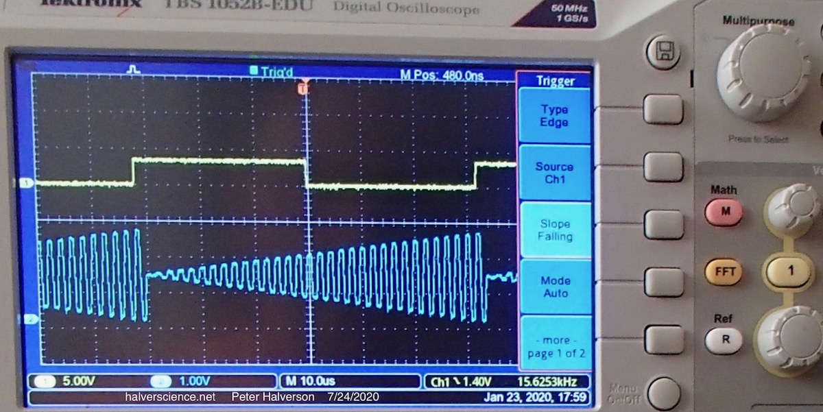
(Technical note regarding digital scopes: The sampling rate advertised on the scope's front panel, 1 Giga-sample/s, would be high enough to display all the waveforms here. But the sample rate is lowered as the horizontal sweep speed is lowered, and for the 15 Hz pattern, it is evidently much less than 500 kHz. 1 Gs/s is what you get at the highest horizontal sweep speed. I wish Tek Scopes told us what sampling rate is being used.)
Video explanation of the thought process and implementation of the 16-bit 1 Ms/s DAC described above.
Using the Linear Technology 2459A (LTC1668) 50 Ms/s DAC
The Linear Technology DAC board uses a parallel interface, so the FPGA sends the data over 16 wires, plus a wire for a clock. The parallel approach is simpler and faster than serial data, but i/o lines are a limited resource.
(I plan to add information here.)