Direct Digital Synthesis
Direct Digital Synthesis (DDS) is a way to generate arbitrary waveforms at (almost) arbitrary frequencies. Extremely low frequencies are easily generated and the frequencies are as accurate as the clock. High frequencies are easily generated, limited only by the speed of the DAC.
DDS opens the door to software defined radio. Amplitude, frequency and phase modulation are very easy to implement. Multiple frequencies with well defined frequency and phases relationships are easily created.
Excellent explanations of DDS are available from Analog Devices here
and here
I will present three examples, in increasing complexity. In this first example the DDS is implemented as follows:
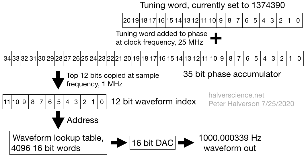
The GoBoard's 25 MHz clock is fed to a 35 bit binary counter.
25 MHz/2**35 = 0.00072760 Hz, so this DDS will have a lowest frequency of 0.00072760 Hz. The output waveform will be generated at 1 million samples/second (1 Ms/s), the rated speed of the Analog Devices AD5541A DAC. The output frequency is the value of the tuning word, M, times the lowest frequency.
To get a particular frequency F, you make M=F/(lowest frequency).
For example, if you want F=2 Hz, M=2/(25000000/2**35) = 2749. Using this tuning word value would give you 2.00016075 Hz.
In the diagram below, a frequency F=1000 Hz is generated, using a tuning word M=1374390.
The waveform is defined by the contents of a ram.ini file. This file must contain 4096 lines, each line having a four hexadecimal digit value in the range of 0000 to ffff. I am providing three examples: sin, triangle and a generic "EKG heartbeat" that I digitized from an EKG image. (To be realistic, run the "EKG" at 1 Hz, to mimic a heart rate of 60 beats/minute.) I am also providing the python code that generated the sin and triangle wave ram.ini files.
DDS Top level module
///////////////////////////////////////////////////////////////////////////////
// File downloaded from https://halverscience.net
///////////////////////////////////////////////////////////////////////////////
// This is a Direct Digital Synthesis arbitrary function generator, frequency range
// 0.000728 Hz to ~200 kHz.  It outputs a sine (typically) or whatever function is in memory.
// The accuracy of the output frequency is dependent on the clock crystal on the
// FPGA board, typically 30 ppm (parts per million).  50 ppm for the GoBoard.
// Waveform values are sent to DAC at 1 MHz.
// Currently uses a Digilent Pmod DA3 DAC, but could be easily adapted to other DACs.
// Author: Peter Halverson 7/2020
///////////////////////////////////////////////////////////////////////////////
`default_nettype none     // Use this to find undeclared wires.  Optional.

module DDS_Function_Generator_Top
  (input  wire i_Clk,         // Main Clock, 25 MHz
   output wire o_Segment1_A, output wire o_Segment1_B, output wire o_Segment1_C,
   output wire o_Segment1_D, output wire o_Segment1_E, output wire o_Segment1_F,
   output wire o_Segment1_G, output wire o_Segment2_A, output wire o_Segment2_B,
   output wire o_Segment2_C, output wire o_Segment2_D, output wire o_Segment2_E,
   output wire o_Segment2_F, output wire o_Segment2_G,
   output wire o_LED_1, output wire o_LED_2, output wire o_LED_3, output wire o_LED_4,
   output wire io_PMOD_1,     // First PMOD connector - not used
   output wire io_PMOD_2,     //
   input  wire io_PMOD_3,     //
   output wire io_PMOD_4,     //
   output wire io_PMOD_7,     // 2nd PMOD connector - has the DAC board.
   output wire io_PMOD_8,     //
   output wire io_PMOD_9,     //
   output wire io_PMOD_10,    //
   input  wire i_Switch_1,    // Wires to the switches.  Not used now, but useful for debugging.
   input  wire i_Switch_2, input  wire i_Switch_3, input  wire i_Switch_4,
   output wire o_VGA_HSync,   // VGA
   output wire o_VGA_VSync,   // I'm using this as a scope trigger line
   output wire o_VGA_Red_0, output wire o_VGA_Red_1, output wire o_VGA_Red_2, output wire o_VGA_Grn_0,
   output wire o_VGA_Grn_1, output wire o_VGA_Grn_2, output wire o_VGA_Blu_0,
   output wire o_VGA_Blu_1, output wire o_VGA_Blu_2
  );

  wire w_Sample_Clock;
  Make_Sample_Clock #(.DIVIDER(25)) Make_Sample_Clock_inst
  (
    .i_Clock(i_Clk),                  // 25 MHz clock in
    .o_Sample_Clock(w_Sample_Clock)   // 1 MHz sample clock out
  );

  parameter NUMBER_OF_POINTS = 4096;
  parameter DATA_WIDTH = 16;  // Our DAC is 16 bits, and the stored waveform has 16 bits.

  wire [DATA_WIDTH-1:0] w_Waveform;

  wire w_Data_Valid;
  Make_Function Make_Function_inst(
    .i_Clk(i_Clk),
    .i_Sample_Clock(w_Sample_Clock),
    .i_Waveform_Index(r_Waveform_Index),
    .o_Waveform(w_Waveform),
    .o_Data_Valid(w_Data_Valid)
  );
                          // Comments apply to the Digilent Pmod DA3.  (The Pmod DA2 is different)
  wire w_Pmod_Port2_Pin1; // ~CS, Pull low when moving data into the DAC
  wire w_Pmod_Port2_Pin2; // DIN Data stream going to the DAC.  16 bits, but 1st 4 bits are always 0.
  wire w_Pmod_Port2_Pin3; // ~LDAC, Falling edge or holding low activates the DAC
  wire w_Pmod_Port2_Pin4; // SCLK, DAC Clock.  Data bits are latched on rising edge of this clock.

  Send_To_DAC_Pmod_DA3 Send_To_DAC_Pmod_DA3_inst(
    .i_Clk(i_Clk),
    .i_Data_Valid(w_Data_Valid),
    .i_DAC_Data(w_Waveform),
    .o_notCS(w_Pmod_Port2_Pin1),
    .o_notLDAC(w_Pmod_Port2_Pin3),
    .o_Sclk(w_Pmod_Port2_Pin4),
    .o_Serial_Data(w_Pmod_Port2_Pin2)
  );

  reg [35-1:0] r_Phase_Accumulator;
  reg [12-1:0] r_Waveform_Index; // 12 bits needed for 4096 points

  // TUNING WORD determines the frequency. Output freq will be
  // (25 MHz / 2**35) * TUNING_WORD = 0.0007275957614183426 Hz * TUNING_WORD
  //
  // Numbers assume the 25 MHz crystal is perfect.
  // Typically, crystals have +/- 50 ppm accuracy, so 25 MHz +/- 1250 Hz
  // Therefore the frequencies below are useful only for comparison to the clock
  // which comes out at the scope trigger
  parameter TUNING_WORD = 1374390;  // Close to 1000 Hz.  Actually 1000.0003385357559 Hz
  //parameter TUNING_WORD = 2749;     // Close to 2 Hz. Actually 2.000160748139024 Hz
  //parameter TUNING_WORD = 1374;     // Close to 1 Hz. Actually 0.9997165761888027 Hz

  always @(posedge i_Clk) begin
    r_Phase_Accumulator = r_Phase_Accumulator + TUNING_WORD;
    r_Waveform_Index <= r_Phase_Accumulator[35-1:23];  // 12 most sig. bits for function lookup
  end //always

  // Make a steady scope trigger for reference and debugging
  reg [18-1:0] r_Scope_Trigger_Counter;  // If I need to divide 25 MHz by 250000, need 18 bits
  reg r_Scope_Trigger;
  always @(posedge i_Clk) begin   //25 MHz clock
    if (r_Scope_Trigger_Counter == 25000-1) begin //250000 for 100 Hz, 25000 for 1000 Hz, etc.
      r_Scope_Trigger_Counter <= 0;
      r_Scope_Trigger <= 1;
    end else begin
      r_Scope_Trigger_Counter <= r_Scope_Trigger_Counter + 1;
      if (r_Scope_Trigger_Counter == 249) r_Scope_Trigger <= 0; //249 would give a 10 us pulse
    end
  end //always
  assign o_VGA_VSync = r_Scope_Trigger;

  // Wires to the DAC
  assign io_PMOD_7  = w_Pmod_Port2_Pin1;//Chip select signal, active low
  assign io_PMOD_1  = w_Pmod_Port2_Pin1;//Duplicate for easier connection to oscilloscope
  assign io_PMOD_8  = w_Pmod_Port2_Pin2;//Serial data out to DAC
  assign io_PMOD_2  = w_Pmod_Port2_Pin2;//Duplicate for easier connection to oscilloscope
  assign io_PMOD_9  = w_Pmod_Port2_Pin3;//~LDAC,  When pulled down, activates the DAC.
                                        //(See AD5541A data sheet)
  assign io_PMOD_10 = w_Pmod_Port2_Pin4;//25 MHz clock to clock in the serial data stream

  assign o_LED_1 = 0;   // Turn off the LEDs  (because they are annoying)
  assign o_LED_2 = 0; assign o_LED_3 = 0; assign o_LED_4 = 0;
  assign o_Segment1_A = 1;assign o_Segment1_B = 1;assign o_Segment1_C = 1;assign o_Segment1_D = 1;
  assign o_Segment1_E = 1;assign o_Segment1_F = 1;assign o_Segment1_G = 1;assign o_Segment2_A = 1;
  assign o_Segment2_B = 1;assign o_Segment2_C = 1;assign o_Segment2_D = 1;assign o_Segment2_E = 1;
  assign o_Segment2_F = 1;assign o_Segment2_G = 1;
endmodule
`default_nettype wire   // Go back to the usual default
Make_Function module
///////////////////////////////////////////////////////////////////////////////
// File downloaded from https://halverscience.net
///////////////////////////////////////////////////////////////////////////////
// This is part of Direct Digital Synthesis arbitrary function generator, frequency range
// 0.000728 Hz to approximately 200 kHz.
// This module reads RAM that has been pre-loaded with the function and delivers
// the 16 bit function value to the top module.
// Author: Peter Halverson 7/2020
///////////////////////////////////////////////////////////////////////////////
`default_nettype none     // Use this to find undeclared wires.  Optional.

module Make_Function
  #(parameter ADDRESS_WIDTH = 12,NUMBER_OF_POINTS = 4096, DATA_WIDTH = 16)
  (
  input wire i_Clk,
  input wire i_Sample_Clock,   // Tells generator to start making the next point
  input wire [ADDRESS_WIDTH-1:0] i_Waveform_Index,   // 14 bits needed to select among
                                            //16384 points.  (4096 points in each quarter wave)
  output wire signed [DATA_WIDTH-1:0] o_Waveform, // Its a 16 bit output, since my DAC is 16 bits
  output wire o_Data_Valid
  );

  reg [ADDRESS_WIDTH-1:0] r_ram_Address;
  reg [DATA_WIDTH-1:0] ram [0:NUMBER_OF_POINTS-1];
  // ram [0:NUMBER_OF_POINTS-1]  works  and ram [NUMBER_OF_POINTS-1:0] should work, but
  // backwards according to the ICEcube2 User Guide.  However, they both work identically.
  initial begin
    $readmemh ("ram_sin.ini", ram);  // Try also ram_triangle.ini and ram_ekg.ini
  end

  reg r_State;
  parameter IDLE_STATE  = 0;  parameter GET_DATA_STATE = 1;

  reg r_Data_Valid;
  reg signed [DATA_WIDTH-1:0] r_Waveform;

  always @(posedge i_Clk) begin
    case (r_State)
      IDLE_STATE: begin
        r_Data_Valid <= 1'b0;
        r_ram_Address <= i_Waveform_Index;
        if (i_Sample_Clock == 1'b1) r_State <= GET_DATA_STATE;
        else r_State <= IDLE_STATE;
      end //IDLE_STATE
      GET_DATA_STATE: begin
        r_Waveform <= ram[r_ram_Address];
        r_Data_Valid <= 1'b1;
        r_State <= IDLE_STATE;
      end //GET_DATA_STATE
      default: r_State <= IDLE_STATE;
    endcase
  end //always

assign o_Waveform   = r_Waveform;
assign o_Data_Valid = r_Data_Valid;
endmodule
`default_nettype wire   // Go back to the usual default
Make_Sample_Clock module
///////////////////////////////////////////////////////////////////////////////
// File downloaded from https://halverscience.net
///////////////////////////////////////////////////////////////////////////////
// This is part of Direct Digital Synthesis arbitrary function generator, frequency range
// 0.000728 Hz to approximately 200 kHz.
// Author: Peter Halverson 7/2020
///////////////////////////////////////////////////////////////////////////////
`default_nettype none     // Use this to find undeclared wires.  Optional.

// This code takes the 25 MHz clock and divides it down to whatever DAC or ADC sampling
// frequency is needed.
// Note the output is NOT symmetric.  It is a 40 ns pulse (1/25 MHz = 40 ns) once every period.

module Make_Sample_Clock #(parameter DIVIDER = 1) //Be sure to pas a valid divider value.  See below.
(
  input wire i_Clock,          // 25 MHz clock in
  output reg o_Sample_Clock
);

// DIVIDER = 25 would give 1 MHz or 1 million DAC updates (samples) per second.
// Note:  at this speed there is noticable distortion on the Pmod DA2 DAC module.
// Slowing it down to 125000 samples/s gives much better results. (Use DIVIDER = 200)
// On the other hand, the Pmod DA3 works fine at 1 million samples/s

  reg [8:0] r_Count;           // 8 bits can handle divider as large as 256
  always @(posedge i_Clock) begin
    if (r_Count == DIVIDER-1) begin
      r_Count <= 0;
      o_Sample_Clock <= 1;
    end else begin
      r_Count <= r_Count + 1;
      o_Sample_Clock <= 0;
    end
  end //always
endmodule
`default_nettype wire   // Go back to the usual default
ram_triangle_generator.py
Python code to generate a triangle wave in Verilog .ini memory initialization format: Each line has one 16 bit word expressed as four hexadecimal digits.
# Python program to crate a hexadecimal encoded table of values that can be read by
# Verilog and used to create a TRIANGLE WAVE lookup table in an FPGA
# (Of course you could easily have the FPGA calculate the waveform... this is just an example.)

# DOWNLOADED FROM https://halverscience.net    Peter Halverson 7/26/2020

from math import *

maximum = 2.0**16 - 1    # Use for 16 bit DACs
imaximum = int(maximum)

ntable = 4096   #Table size, 2**12, just fits into the GoBoard's iCE40 HX1K VQ100 memory
itriangle_table = []  #Creates an empty array

for itable in range(0,ntable/2+1):
  x = imaximum*itable*2.0/ntable
  itriangle_table=itriangle_table+[int(round(x))]
  print itable," ",x

for itable in range(ntable/2+1,ntable):
  x = imaximum - imaximum*(itable-ntable/2.0)*2.0/ntable
  itriangle_table=itriangle_table+[int(round(x))]
  print itable," ",x

print "///////////////////////////////////////////////////////////////////////////"

print_hex_values = True #Use False for debugging, True to get the hex numners fror the table
#Copy/paste or pipe ">" this output into a verilog memory initialization file
debugging = False
if print_hex_values:
  for i in range(0,ntable):
    d=itriangle_table[i]
    if debugging: print i,",",d
    else:
      # s is the string that will have the hex data.
      s = '{:04x}'.format(d)
      print s
ram_sin_generator.py
Python code to generate a sine wave in Verilog .ini memory initialization format: Each line has one 16 bit word expressed as four hexadecimal digits.
# Python program to crate a hexadecimal encoded table of values that can be read by
# Verilog and used to create a sine wave lookup table in an FPGA

# DOWNLOADED FROM https://halverscience.net    Peter Halverson 7/26/2020

from math import *

maximum = 2.0**16 - 1    # Use for 16 bit DACs
imaximum = int(maximum)

ntable = 4096   #Table size, 2**12, just fits into the GoBoard's iCE40 HX1K VQ100 memory
isin_table = []  #Creates an empty array
for itable in range(0,ntable+1):
  x = 2.0*pi*itable/ntable     #x is in radians
  isin_table = isin_table + [int(round(imaximum*(1.0+sin(x))/2.0))] #Fill the array

most_positive_error = 0.0
most_negative_error = 0.0
most_positive_error_i = 0
most_negative_error_i = 0

npoints = ntable           #This will be a full cycle, 2*pi radians
for i in range(0,npoints+1):
  x = 2.0*pi*i/npoints     #x is in radians
  true_sin = maximum*(1.0+sin(x))/2.0
  fpga_sin = isin_table[i]
  error = fpga_sin-true_sin

  print "i=%4i"%i,"x=%5.3f"%x,"truth=%8.2f"%true_sin,
  print "fpga=%6i"%fpga_sin,"err=%7.2f"%error

  if error > most_positive_error:
    most_positive_error = error
    most_positive_error_i = i
  if error < most_negative_error:
    most_negative_error = error
    most_negative_error_i = i

print "most_positive_error =",most_positive_error,"at i=",most_positive_error_i
print "most_negative_error =",most_negative_error,"at i=",most_negative_error_i

print_hex_values = True  #Copy/paste or pipe ">" this output into a verilog memory initialization file
debugging = False
if print_hex_values:
  for i in range(0,npoints):
    d=isin_table[i]
    if debugging: print i,",",d
    else:
      # s is the string that will have the hex data.
      s = '{:04x}'.format(d)
      print s