Improved (again) Function Generator
Compared to the first version
- The lowest frequency (and the frequency steps) have been made more user-friendly: 1 milli Hertz. That means if you want 123 Hz, the tuning word should be 123000.
- To make this possible, in spite of a 25 MHz clock that can't be changed, the number of samples in a full cycle has been changed, from 4096 to 3406. Also, the update rate of the phase accumulator is 25 MHz / 7 = 3.5714... MHz. This was done because 25 MHz/(7 * 3406 * 2**20)=0.001 Hz. Approximately. It is actually 0.000999994 Hz.
- This version can be controlled via the serial port. The FPGA uses the NandLand UART receiver code and parses human-compatible base-ten numbers and recognises three commands:
- "a" to set the amplitude
- "f" to set the frequency
- "p" to add/or subtract phase
- Relative to the 2nd version, the buttons have been removed. Why? See next bullet.
- This version uses all of the resources in the Lattice iCE40 HX1K VQ100 chip used on the GoBoard. If you want more capabilites, you have to step up to a more powerful FPGA. (Discussion on the Hardware page.)
- Relative to the 2nd version, the requirement for symmetry is gone. Any waveform shape is OK.
Serial Interface Control
As explained in the NanLand exposition on UARTs, you can communicate with the FPGA via a serial terminal. On Windows you could use TeraTerm and since I use Ubuntu Linux, I use GTKTerm. See the LINUX NOTES page on this site for installation of gGTKTerm.
The Verilog UART code is currently set to 1200 baud, which is deliberately slow to properly echo each character when copy-pasting commands.
The command format is number - command. Examples:
1000f      //Set frequency to 1000 milliHertz, i.e. 1 Hz
440000f    //Set frequency to 440 Hz, "A" in music.

//Just for fun try this:  G3 207.652 Hz E4 329.628 Hz  C4 261.626 Hz,
//as quickly as you can copy-paste
207652f
329628f
261626f

0a           //Set amplitude to zero.  The waveform goes away.
32767a       //Set amplitude to maximum.   (Just for fun, try 50000a)

223215616p   //Advance the phase relative to the scope trigger by 22.5 degrees
3348234240p  //Retard the phase by 22.5 degrees.
(The FPGA does not understand "//" to mean comments. Leave my comments out.)
For the phase control ote that 360 degrees is 3571449856 counts in the phase accumulator That number is 13624 * 2**18. (The size of the waveform memory times the number of counts needed to make the phase accumulator roll-over.)
Useful phases:
One degree       9920694
22.5 deg:        223215616
45 deg:          446431232
90 deg:          892862464
180 deg:         1785724928
-1 = 359 deg:    3561529162
-22.5=337.5 deg: 3348234240
-45=315 deg:     3125018624
-90=270 deg:     2678587392
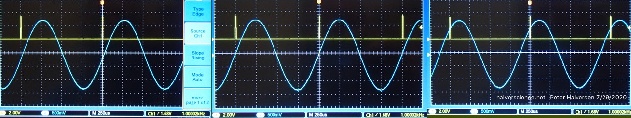
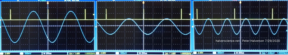
Example command dialog
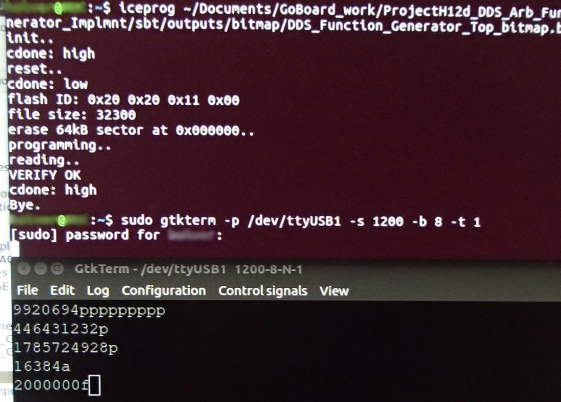
In the GtkTerm window there are five commands lines. Here is what they did:
- One degree phase shift, repeated 9 times.
- +45 degree phase shift.
- 180 degree phase shift. On the scope it looks like the sine flipped + and -.
- Reduce the amplitude to 1/2 of full scale.
- Set the frequency to 2 kHz.
DDS Top level module
///////////////////////////////////////////////////////////////////////////////
// File downloaded from https://halverscience.net
///////////////////////////////////////////////////////////////////////////////
// This is a Direct Digital Synthesis function generator, frequency range
// 0.001 Hz to ~200 kHz.  It outputs a sine though that can be changed by
// loading memory with different numbers.
// The accuracy of the output frquency is dependent on the clock crystal on the
// FPGA board, 50 ppm (parts per million) on the GoBoard.
// Author: Peter Halverson 7/2020
///////////////////////////////////////////////////////////////////////////////

// Arbitrary function generator with "human-friendly" 1 mHz frequency increments.

// This version tries to be more user-friendly by making the lowest frequency, i.e. the frequency
// step size, be very close to 1 milli-Hertz.
// The is achieved by dividing the 25 MHz clock by 7 and making the waveform memory be 3406 words
// long.   The divider is 20 bits.
// The lowest frequency is (25 MHz / 7)/(2**20 * 3406) = 0.00099999404 Hz, very close to 1 mHz.
// Waveform values are sent to DAC at 1 MHz.
// Currently uses a Digilent Pmod DA3 DAC, but could be easily adapted to other DACs.

// In this version the frequency and phase can be controlled via the serial port.
// See NandLand.com for explanations regarding the serial port.
// The USB programming port can also act as a serial port.
// On my Ubuntu Linux system, the terminal command to talk to the serial port is
// sudo gtkterm -p /dev/ttyUSB1 -s 1200 -b 8 -t 1
// I am using 1200 baud (which is slow) because at 115200 baud some of the echoed characters were
// getting lost.  It didn't change the performance but it looked strange.  Could fix this
// problem by implementing a character buffer.
`default_nettype none     // Use this to find undeclared wires.  Optional.

module DDS_Function_Generator_Top
  (input  wire i_Clk,         // Main Clock, 25 MHz
   input  wire i_UART_RX,   // UART RX Data.  This data comes from your keyboard.
   output wire o_UART_TX,   // UART TX Data.  This data goes to your computer screen.
   output wire o_Segment1_A, output wire o_Segment1_B, output wire o_Segment1_C,
   output wire o_Segment1_D, output wire o_Segment1_E, output wire o_Segment1_F,
   output wire o_Segment1_G, output wire o_Segment2_A, output wire o_Segment2_B,
   output wire o_Segment2_C, output wire o_Segment2_D, output wire o_Segment2_E,
   output wire o_Segment2_F, output wire o_Segment2_G,
   output wire o_LED_1, output wire o_LED_2, output wire o_LED_3, output wire o_LED_4,
   output wire io_PMOD_1,     // First PMOD connector - not used
   output wire io_PMOD_2,     //
   input  wire io_PMOD_3,     //
   output wire io_PMOD_4,     //
   output wire io_PMOD_7,     // 2nd PMOD connector - has the DAC board.
   output wire io_PMOD_8,     //
   output wire io_PMOD_9,     //
   output wire io_PMOD_10,    //
   input  wire i_Switch_1, input wire i_Switch_2, input wire i_Switch_3,input wire i_Switch_4,
   output wire o_VGA_HSync,   // VGA
   output wire o_VGA_VSync,   // Scope trigger line
   output wire o_VGA_Red_0, output wire o_VGA_Red_1, output wire o_VGA_Red_2,
   output wire o_VGA_Grn_0, output wire o_VGA_Grn_1, output wire o_VGA_Grn_2,
   output wire o_VGA_Blu_0, output wire o_VGA_Blu_1, output wire o_VGA_Blu_2
  );

  reg r_Phase_Accumulator_Clock; // Will be 25 MHz / 7 = 3.571 MHz
  reg [3-1:0] r_Phase_Accumulator_Clock_Counter;  // 7 needs 3 bits
  always @(posedge i_Clk) begin
    if (r_Phase_Accumulator_Clock_Counter == 7-1) begin
      r_Phase_Accumulator_Clock_Counter <= 0;
      r_Phase_Accumulator_Clock <= 1'b1;
    end else begin
      r_Phase_Accumulator_Clock_Counter <= r_Phase_Accumulator_Clock_Counter + 1;
      r_Phase_Accumulator_Clock <= 1'b0;
    end
  end //always

  wire w_Sample_Clock;
  Make_Sample_Clock #(.DIVIDER(25)) Make_Sample_Clock_inst (
    .i_Clk(i_Clk),                  // 25 MHz clock in
    .o_Sample_Clock(w_Sample_Clock)   // 1 MHz sample clock out
  );

  parameter NUMBER_OF_POINTS = 3406; // Length of the waveform stored in memory.
  parameter DATA_WIDTH = 16;  // Our DAC is 16 bits, and the stored waveform has 16 bits.

  wire signed [DATA_WIDTH-1:0] ws_Waveform;  //"signed" means the msb is used as a sign bit
  wire [DATA_WIDTH-1:0]         w_Waveform;  //  This is unsigned

  //Implement an adjustable amplitude;
  reg signed [2*DATA_WIDTH-1:0] rs_Waveform_Mult_by_A;
  reg signed [DATA_WIDTH-1+1:0] rs_Amplitude;  // 100% will be represented by 2**15.
                              // Sign takes an extra bit, even though it is always zero.
  // This looks like I'm using one more bit than needed
  // but I didn't want to lose accuracy by multiplying by 2**15 - 1
  reg r_Data_Valid_Holder; //To get the timing right; the amplitude adjustment
                           //takes an extra clock cycle.

  wire w_Data_Valid;
  Make_Function #(.ADDRESS_WIDTH(12),.NUMBER_OF_POINTS(NUMBER_OF_POINTS),.DATA_WIDTH(DATA_WIDTH))
  Make_Function_inst (
    .i_Clk(i_Clk),
    .i_Sample_Clock(w_Sample_Clock),
    .i_Waveform_Index(w_Waveform_Index),
    .o_Waveform(ws_Waveform),
    .o_Data_Valid(w_Data_Valid)
  );

  // ------------- Use these if NOT using amplitude adjustment
  //assign w_Waveform[14:0] = ws_Waveform[14:0];
  //assign w_Waveform[15] = ~ws_Waveform[15]; //sign bit, flipped to behave like unsigned

  // ------------- Use these if you ARE using amplitude adjustment
  assign w_Waveform[14:0] = rs_Waveform_Mult_by_A[29:15]; //15 bits of the sine multiplied by the amplitude.
  // Note that bit 30 is not used.  (I had to think very carefully about that!!)
  assign w_Waveform[15] = ~rs_Waveform_Mult_by_A[31]; //sign bit, flipped to behave like unsigned

  always @(posedge i_Clk) begin
    r_Data_Valid_Holder <= w_Data_Valid;   // Delay the data valid flag to match the
    // delay introduced by the amplitude adjustment steps.
    // Adjust the amplitude sent to the DAC
    rs_Waveform_Mult_by_A <= ws_Waveform*rs_Amplitude;
  end //always

                          // Comments apply to the Pmod DA3.  (The Pmod DA2 is different)
  wire w_Pmod_Port2_Pin1; // ~CS, Pull low when moving data into the DAC
  wire w_Pmod_Port2_Pin2; // DIN Data stream going to the DAC.  16 bits.
  wire w_Pmod_Port2_Pin3; // ~LDAC, Falling edge or holding low activates the DAC
  wire w_Pmod_Port2_Pin4; // SCLK, DAC Clock.  Data bits are latched on rising edge of this clock.

  Send_To_DAC_Pmod_DA3
  Send_To_DAC_Pmod_DA3_inst(
    .i_Clk(i_Clk),
    //.i_Data_Valid(w_Data_Valid),  //Use if NOT using amplitude adjustment
    .i_Data_Valid(r_Data_Valid_Holder),//Use if you ARE using amplitude adjustement
    .i_DAC_Data(w_Waveform),
    .o_notCS(w_Pmod_Port2_Pin1),
    .o_notLDAC(w_Pmod_Port2_Pin3),
    .o_Sclk(w_Pmod_Port2_Pin4),
    .o_Serial_Data(w_Pmod_Port2_Pin2)
  );

  // TUNING WORD determines the frequency.  Output freq will be close to 0.001 Hz * TUNING_WORD
  // (Actually the output frequency is [(25.e6/(7*4*3406*2**18) = 0.00099999404 Hz] * TUNING_WORD)
  // Numbers assume the 25 MHz crystal is perfect.
  // Typically, crystals have +/- 30 ppm accuracy, so 25 MHz +/- 750 Hz  (I need to check this)
  // Therefore the frequencies below are useful only for comparison to the clock
  // which comes out at the scope trigger
  // parameter TUNING_WORD_START = 100000000;  // Close to 100 kHz.  Actually 99999.4040356 Hz
  // parameter TUNING_WORD_START = 100000000+596;  // Very close to 100 kHz  Actually 100000.0000356 Hz
  // parameter TUNING_WORD_START = 1000000;  //  Close to 1 kHz.  Actually 999.994040356 Hz
  parameter TUNING_WORD_START = 1000000+6;  //  Very close to 1 kHz.  Actually 1000.000040356 Hz

  // Implement an adjustable frequency.  Now TUNING_WORD specifies the initial frequency.
  reg [32-1:0] r_Tuning_Word = 0;

  reg [8-1:0] r_Power_On = 0;  // Used to wait until the FPGA is fully on and functional

  reg [33-1:0] r_Phase_Accumulator;// Need 32 bits +1 extra for large tuning words
  wire [12-1:0] w_Waveform_Index; // Need enough bits to address NUMBER_OF_POINTS
  assign w_Waveform_Index = r_Phase_Accumulator[32-1:21-1];
  parameter PHASE_ACCUM_MAX = NUMBER_OF_POINTS * 2**20;
  reg [33-1:0] r_Next_Phase;  //Need 32 bits +1 extra for large tuning words
  reg [32-1:0] r_Phase_Adjust = 0;
  always @(posedge r_Phase_Accumulator_Clock) begin
    if (r_Power_On == 8'hff) begin
      if (r_Next_Phase > PHASE_ACCUM_MAX-1) begin    // If true,then phase wraps around
        r_Phase_Accumulator <= r_Next_Phase - PHASE_ACCUM_MAX;
        r_Next_Phase <= r_Next_Phase - PHASE_ACCUM_MAX + r_Tuning_Word + r_Phase_Adjust;
      end else begin
        r_Phase_Accumulator <= r_Next_Phase;
        r_Next_Phase <= r_Next_Phase + r_Tuning_Word + r_Phase_Adjust;
      end
      case (r_Command_From_Serial)
        SET_FREQUENCY: begin
          r_Tuning_Word <= r_Binary_Number; //r_Data_From_Serial;
          r_Command_From_Serial_Accepted <= 1'b1;
        end //SET_FREQUENCY
        CHANGE_PHASE: begin
          r_Phase_Adjust <= r_Binary_Number; //r_Data_From_Serial;
          r_Command_From_Serial_Accepted <= 1'b1;
        end //CHANGE_PHASE
        SET_AMPLITUDE: begin
          rs_Amplitude[15:0] <= r_Binary_Number[15:0]; //r_Data_From_Serial[14:0];
          r_Command_From_Serial_Accepted <= 1'b1;
        end //SET_AMPLITUDE
        default: begin
          r_Command_From_Serial_Accepted <= 1'b0;
          r_Phase_Adjust <= 0;
        end //default
      endcase
    end else begin   // The FPGA is (perhaps) not yet fully on.  Wait a little longer.
      // Note: it seems LSE doesn't implement initialized registers, except for zeroing at power-up.
      r_Power_On <= r_Power_On + 1'b1;  // Keep looping while the FPGA starts up.
      // Initialize various things while waiting for FPGA to start.
      r_Tuning_Word <= TUNING_WORD_START;  // Set the initial freq
      rs_Amplitude <= 2**15;//Use if you ARE using amplitude adj. Set A to 100%
      r_Phase_Adjust <= 0;                 // Set phase change to 0
      r_Command_From_Serial_Accepted <= 1'b0;
    end //if
  end //always

  // Notes on computing the phase changes:
  // One full cycle, 360 degrees is 3406 * 2**20 counts on the phase accumulator
  // Hence, to advance phase 1 degrees, set r_Phase_Adjust = (3406 * 2**20)/360
  //                                                       = 9920694.044 (round, of course)
  // 22.5 deg:223215616 45 deg:446431232  90 deg:892862464  180 deg:1785724928
  // -22.5=337.5 deg:3348234240   -45=315 deg:3125018624  -90=270 deg:2678587392

  // Make a steady scope trigger for reference and debugging
  reg [18-1:0] r_Scope_Trigger_Counter;  // If I need to divide 25 MHz by 250000, need 18 bits
  reg r_Scope_Trigger;
  always @(posedge i_Clk) begin   //25 MHz clock
    if (r_Scope_Trigger_Counter == 25000-1) begin //250000 for 100 Hz, 25000 for 1000 Hz, etc.
      r_Scope_Trigger_Counter <= 0;
      r_Scope_Trigger <= 1;
    end else begin
      r_Scope_Trigger_Counter <= r_Scope_Trigger_Counter + 1;
      if (r_Scope_Trigger_Counter == 249) r_Scope_Trigger <= 0; //249 would give a 10 microsec pulse
    end
  end //always
  assign o_VGA_VSync = r_Scope_Trigger;

  // =================== Serial port control of signal generator =======================
  reg [32-1:0] r_Tuning_Word_From_Serial = 0;
  //reg r_Tuning_Word_From_Serial_Accepted = 0;  // Handshake for Tuning_Word
  reg [32-1:0] r_Phase_Adjust_From_Serial = 0;
  //reg r_Phase_Adjust_From_Serial_Accepted = 0;  // Handshake for Phase_Adjust
  wire w_RX_DV; // True when incoming ascii is valid
  wire [7:0] w_RX_Byte;
  wire w_TX_Active, w_TX_Serial;
  reg [7:0] r_TX_Byte;  //Used to send ASCII back to the screen.
  reg r_TX_DV; // Set to true when outgoing ASCII is valid.
  reg [4-1:0] r_BCD_input;   // Numbers from keyboard, converted to binary 0,1,2..9
  reg [4-1:0] r_Digit_Count;  // Which digit are we getting?
  reg [32-1:0] r_Binary_Number; // Based ten number from serial port converted to binary or hexadecimal
  //reg [32-1:0] r_Data_From_Serial=0;
  reg [2-1:0] r_Command_From_Serial=0;
  reg r_Command_From_Serial_Accepted = 0;
  parameter SET_FREQUENCY = 1; parameter CHANGE_PHASE = 2; parameter SET_AMPLITUDE = 3;
  reg [2-1:0] r_State;     // For state machine
  parameter GET_CHARACTER = 0; parameter BUILD_NUMBER = 1; parameter CLEAN_UP = 2;
  always @(posedge i_Clk) begin  //Note that this loop runs full speed, 25 MHz, but
    // the function generator loop runs more slowly.  Hence to make the commands and
    // data go from here to there requires careful handshaking.
    case (r_State)
      GET_CHARACTER: begin
        if (w_RX_DV == 1'b1) begin
          if ((w_RX_Byte >= 8'h30) && (w_RX_Byte <= 8'h39)) begin//Check if "0", "1",... "9"
            // "0" is hex 30, "1" is hex 31 etc.
            r_TX_Byte <= w_RX_Byte;  //Echo the character on screen
            r_TX_DV <= 1'b1;
            r_BCD_input <= w_RX_Byte - 8'h30;
            r_Digit_Count <= r_Digit_Count + 1;
            r_State <= BUILD_NUMBER;
          end else begin
            case (w_RX_Byte)
            8'h0D :begin   // CR (Enter) character
              r_Digit_Count <= 0;
              r_TX_Byte <= 8'h0D;  //Send CR to screen
              r_TX_DV <= 1'b1;
              // Do nothing.
              r_State <= CLEAN_UP;
            end //CR
            8'h66: begin   //"f"
              r_Command_From_Serial = SET_FREQUENCY;
              r_Digit_Count <= 0;
              r_TX_Byte <= 8'h66;  //Send "f" to screen
              r_TX_DV <= 1'b1;
              r_State <= CLEAN_UP;
            end  // "f"
            8'h70:  begin   // "p"
              r_Command_From_Serial <= CHANGE_PHASE;
              r_Digit_Count <= 0;
              r_TX_Byte <= 8'h70;  //Send "p" to screen
              r_TX_DV <= 1'b1;
              r_State <= CLEAN_UP;
            end //"p"
            8'h61: begin   // "a"
              r_Command_From_Serial <= SET_AMPLITUDE;
              r_Digit_Count <= 0;
              r_TX_Byte <= 8'h61;  //Send "a" to screen
              r_TX_DV <= 1'b1;
              r_State <= CLEAN_UP;
            end //"a"
            default: r_State <= 0;
            endcase
          end //if
        end else begin
          if ((r_TX_Byte == 8'h0D) && (w_TX_Active == 1'b0)) begin
            r_TX_Byte <= 8'h0A;  // Send a linefeed character
            r_TX_DV <= 1'b1;
            r_State <= CLEAN_UP;
          end
          if (r_Command_From_Serial_Accepted == 1'b1) begin
            r_Command_From_Serial <= 0;
          end //if
        end  //if
      end //GET_CHARACTER
      BUILD_NUMBER: begin
        r_TX_DV <= 1'b0;
        if (r_Digit_Count == 1) begin
          r_Binary_Number[32-1:4] = 28'h0000000;
          r_Binary_Number[3:0] <= r_BCD_input;  // Start with just zeroes and the number
          r_State <= GET_CHARACTER;
        end else begin
          r_Binary_Number <= r_Binary_Number*10 + r_BCD_input;
          r_State <= GET_CHARACTER;
        end //if
        if (r_Command_From_Serial_Accepted == 1'b1) begin
          r_Command_From_Serial <= 0;
        end //if
      end //BUILD_NUMBER
      CLEAN_UP: begin
        r_TX_DV <= 1'b0;
        r_State <= GET_CHARACTER;
        if (r_Command_From_Serial_Accepted == 1'b1) begin
          r_Command_From_Serial <= 0;
        end //if
      end //CLEAN_UP
      default:  r_State <= GET_CHARACTER;
    endcase
    //if (r_Tuning_Word_From_Serial_Accepted == 1'b1) r_Tuning_Word_From_Serial <= 0;   //Handshake for Tuning_Word
    //if (r_Phase_Adjust_From_Serial_Accepted == 1'b1) r_Phase_Adjust_From_Serial <= 0; //Handshake for Phase_Adjust
  end //always

// 115200 baud: 25.e6/115200 = 217
// 9600   Baud: 25.e6/9600   = 2604
// 2400   Baud: 25.e6/2400   = 10417
// 1200   Baud: 25.e6/1200   = 20833   <------ recommended for copy/paste into serial terminal.
// 300   Baud:  25.e6/300    = 83333   Need 17 bits

  UART_RX #(.CLKS_PER_BIT(20833)) UART_RX_Inst
  (.i_Clk(i_Clk),
   .i_RX_Serial(i_UART_RX),
   .o_RX_DV(w_RX_DV),
   .o_RX_Byte(w_RX_Byte));

  UART_TX #(.CLKS_PER_BIT(20833)) UART_TX_Inst
  (.i_Clk(i_Clk),
   .i_TX_DV(r_TX_DV),
   .i_TX_Byte(r_TX_Byte),
   .o_TX_Active(w_TX_Active),
   .o_TX_Serial(w_TX_Serial),
   .o_TX_Done());

  // Drive UART line high when transmitter is not active
  assign o_UART_TX = w_TX_Active ? w_TX_Serial : 1'b1;
  // =================== END Serial Port code ==========================================

// Turn LEDs off
   assign o_Segment1_A = 1'b1; assign o_Segment1_B = 1'b1; assign o_Segment1_C = 1'b1;
   assign o_Segment1_D = 1'b1; assign o_Segment1_E = 1'b1; assign o_Segment1_F = 1'b1;
   assign o_Segment1_G = 1'b1; assign o_Segment2_A = 1'b1; assign o_Segment2_B = 1'b1;
   assign o_Segment2_C = 1'b1; assign o_Segment2_D = 1'b1; assign o_Segment2_E = 1'b1;
   assign o_Segment2_F = 1'b1; assign o_Segment2_G = 1'b1;

  // Wires to the DAC
  assign io_PMOD_7  = w_Pmod_Port2_Pin1;//Chip select signal, active low
  assign io_PMOD_1  = w_Pmod_Port2_Pin1;//Duplicate for easier connection to oscilloscope
  assign io_PMOD_8  = w_Pmod_Port2_Pin2;//Serial data out to DAC
  assign io_PMOD_2  = w_Pmod_Port2_Pin2;//Duplicate for easier connection to oscilloscope
  assign io_PMOD_9  = w_Pmod_Port2_Pin3;//~LDAC,  When pulled down, activates the DAC.
                                        //(See AD5541A data sheet)
  assign io_PMOD_10 = w_Pmod_Port2_Pin4;//25 MHz clock to clock in the serial data stream
  endmodule
`default_nettype wire   // Go back to the usual default
Make_Function module
///////////////////////////////////////////////////////////////////////////////
// File downloaded from http://halverscience.net
///////////////////////////////////////////////////////////////////////////////
// This module generates a waveform, typically a sin though that can be changed by
// loading memory with different numbers. The user must provide an x value in the range of 0 to
// NUMBER_OF_POINTS - 1 and the module returns a 16 bit signed y value in the range of
// -(2**15-1) to + 2**15-1.
// Author: Peter Halverson 7/2020
///////////////////////////////////////////////////////////////////////////////
`default_nettype none     // Use this to find undeclared wires.  Optional.

module Make_Function
  #(parameter ADDRESS_WIDTH=0,     // 12 bits is enough for 3406 points
     NUMBER_OF_POINTS=0,           // 3406
     DATA_WIDTH=0)                 // Should be 16, to match 16 bit DAC
  (
  input wire i_Clk,
  input wire i_Sample_Clock,       // Tells generator to start making the next point
  input wire [ADDRESS_WIDTH-1:0] i_Waveform_Index, // Specifies which point to get from RAM
  output wire signed [DATA_WIDTH-1:0] o_Waveform,
  output wire o_Data_Valid
  );

  reg [ADDRESS_WIDTH-1:0] r_ram_Address;
  reg [DATA_WIDTH-1:0] ram [0:NUMBER_OF_POINTS-1];
  initial begin
    $readmemh ("ram_sin.ini", ram);  // Read the function
  end

  reg r_State;
  parameter IDLE_STATE  = 0;  parameter READ_MEMORY_STATE = 1;

  reg r_Data_Valid;
  reg signed [DATA_WIDTH-1:0] r_Waveform;
  always @(posedge i_Clk) begin
    case (r_State)
      IDLE_STATE: begin
        r_Data_Valid <= 1'b0;
        r_ram_Address <= i_Waveform_Index;  // Grab the address before it changes
        if (i_Sample_Clock == 1'b1) r_State <= READ_MEMORY_STATE;
        else r_State <= IDLE_STATE;
      end //IDLE_STATE
      READ_MEMORY_STATE: begin
        r_Waveform <= ram[r_ram_Address];
        r_Data_Valid <= 1'b1;
        r_State <= IDLE_STATE;
      end //READ_MEMORY_STATE
      default: r_State <= IDLE_STATE;
    endcase
  end //always
  assign o_Waveform   = r_Waveform;
  assign o_Data_Valid = r_Data_Valid;
endmodule
`default_nettype wire   // Go back to the usual default
Make_Sample_Clock module
Same as on the DDS Function Generator page.
Send_To_DAC_Pmod_DA3
Same as on the Analog Output page.
UART_RX module
// File Downloaded from http://www.nandland.com
/////////////////////////////////////////////////////////////////////
// This file contains the UART Receiver.  This receiver is able to
// receive 8 bits of serial data, one start bit, one stop bit,
// and no parity bit.  When receive is complete o_rx_dv will be
// driven high for one clock cycle.
//
// Set Parameter CLKS_PER_BIT as follows:
// CLKS_PER_BIT = (Frequency of i_Clk)/(Frequency of UART)
// Example: 25 MHz Clock, 115200 baud UART
// (25000000)/(115200) = 217

// 9600 Baud: 25.e6/9600 = 2604
// 2400 Baud: 25.e6/2400 = 10417.
// 1200 Baud: 25.e6/1200 = 20833
// 300 Baud:  25.e6/300  = 83333.   Need 17 bits

module UART_RX
  #(parameter CLKS_PER_BIT = 217)(
   input        i_Clk,
   input        i_RX_Serial,
   output       o_RX_DV,
   output [7:0] o_RX_Byte
   );

  parameter IDLE         = 3'b000;
  parameter RX_START_BIT = 3'b001;
  parameter RX_DATA_BITS = 3'b010;
  parameter RX_STOP_BIT  = 3'b011;
  parameter CLEANUP      = 3'b100;

  reg [17-1:0]     r_Clock_Count = 0;    // 17 bits needed for 300 baud
  reg [2:0]     r_Bit_Index   = 0; //8 bits total
  reg [7:0]     r_RX_Byte     = 0;
  reg           r_RX_DV       = 0;
  reg [2:0]     r_SM_Main     = 0;


  // Purpose: Control RX state machine
  always @(posedge i_Clk)
  begin
    case (r_SM_Main)
      IDLE :
        begin
          r_RX_DV       <= 1'b0;
          r_Clock_Count <= 0;
          r_Bit_Index   <= 0;

          if (i_RX_Serial == 1'b0)          // Start bit detected
            r_SM_Main <= RX_START_BIT;
          else
            r_SM_Main <= IDLE;
        end

      // Check middle of start bit to make sure it's still low
      RX_START_BIT :
        begin
          if (r_Clock_Count == (CLKS_PER_BIT-1)/2)
          begin
            if (i_RX_Serial == 1'b0)
            begin
              r_Clock_Count <= 0;  // reset counter, found the middle
              r_SM_Main     <= RX_DATA_BITS;
            end
            else
              r_SM_Main <= IDLE;
          end
          else
          begin
            r_Clock_Count <= r_Clock_Count + 1;
            r_SM_Main     <= RX_START_BIT;
          end
        end // case: RX_START_BIT


      // Wait CLKS_PER_BIT-1 clock cycles to sample serial data
      RX_DATA_BITS :
        begin
          if (r_Clock_Count < CLKS_PER_BIT-1)
          begin
            r_Clock_Count <= r_Clock_Count + 1;
            r_SM_Main     <= RX_DATA_BITS;
          end
          else
          begin
            r_Clock_Count          <= 0;
            r_RX_Byte[r_Bit_Index] <= i_RX_Serial;

            // Check if we have received all bits
            if (r_Bit_Index < 7)
            begin
              r_Bit_Index <= r_Bit_Index + 1;
              r_SM_Main   <= RX_DATA_BITS;
            end
            else
            begin
              r_Bit_Index <= 0;
              r_SM_Main   <= RX_STOP_BIT;
            end
          end
        end // case: RX_DATA_BITS


      // Receive Stop bit.  Stop bit = 1
      RX_STOP_BIT :
        begin
          // Wait CLKS_PER_BIT-1 clock cycles for Stop bit to finish
          if (r_Clock_Count < CLKS_PER_BIT-1)
          begin
            r_Clock_Count <= r_Clock_Count + 1;
          r_SM_Main     <= RX_STOP_BIT;
          end
          else
          begin
             r_RX_DV       <= 1'b1;
            r_Clock_Count <= 0;
            r_SM_Main     <= CLEANUP;
          end
        end // case: RX_STOP_BIT


      // Stay here 1 clock
      CLEANUP :
        begin
          r_SM_Main <= IDLE;
          r_RX_DV   <= 1'b0;
        end


      default :
        r_SM_Main <= IDLE;

    endcase
  end

  assign o_RX_DV   = r_RX_DV;
  assign o_RX_Byte = r_RX_Byte;

endmodule // UART_RX
Reproduced with permission from NandLand.
UART_TX module
//////////////////////////////////////////////////////////////////////
// File Downloaded from http://www.nandland.com
//////////////////////////////////////////////////////////////////////
// This file contains the UART Transmitter.  This transmitter is able
// to transmit 8 bits of serial data, one start bit, one stop bit,
// and no parity bit.  When transmit is complete o_Tx_done will be
// driven high for one clock cycle.
//
// Set Parameter CLKS_PER_BIT as follows:
// CLKS_PER_BIT = (Frequency of i_Clk)/(Frequency of UART)
// Example: 25 MHz Clock, 115200 baud UART
// (25000000)/(115200) = 217

// 9600 Baud: 25.e6/9600 = 2604
// 2400 Baud: 25.e6/2400 = 10417.
// 1200 Baud: 25.e6/1200 = 20833
// 300 Baud:  25.e6/300  = 83333.   Need 17 bits

module UART_TX
  #(parameter CLKS_PER_BIT = 217)
  (
   input       i_Clk,
   input       i_TX_DV,
   input [7:0] i_TX_Byte,
   output      o_TX_Active,
   output reg  o_TX_Serial,
   output      o_TX_Done
   );

  parameter IDLE         = 3'b000;
  parameter TX_START_BIT = 3'b001;
  parameter TX_DATA_BITS = 3'b010;
  parameter TX_STOP_BIT  = 3'b011;
  parameter CLEANUP      = 3'b100;

  reg [2:0] r_SM_Main     = 0;
  reg [17-1:0] r_Clock_Count = 0;  // 17 bits needed for 300 baud
  reg [2:0] r_Bit_Index   = 0;
  reg [7:0] r_TX_Data     = 0;
  reg       r_TX_Done     = 0;
  reg       r_TX_Active   = 0;

  always @(posedge i_Clk)
  begin
    case (r_SM_Main)
      IDLE :
        begin
          o_TX_Serial   <= 1'b1;         // Drive Line High for Idle
          r_TX_Done     <= 1'b0;
          r_Clock_Count <= 0;
          r_Bit_Index   <= 0;

          if (i_TX_DV == 1'b1)
          begin
            r_TX_Active <= 1'b1;
            r_TX_Data   <= i_TX_Byte;
            r_SM_Main   <= TX_START_BIT;
          end
          else
            r_SM_Main <= IDLE;
        end // case: IDLE

      // Send out Start Bit. Start bit = 0
      TX_START_BIT :
        begin
          o_TX_Serial <= 1'b0;

          // Wait CLKS_PER_BIT-1 clock cycles for start bit to finish
          if (r_Clock_Count < CLKS_PER_BIT-1)
          begin
            r_Clock_Count <= r_Clock_Count + 1;
            r_SM_Main     <= TX_START_BIT;
          end
          else
          begin
            r_Clock_Count <= 0;
            r_SM_Main     <= TX_DATA_BITS;
          end
        end // case: TX_START_BIT

      // Wait CLKS_PER_BIT-1 clock cycles for data bits to finish
      TX_DATA_BITS :
        begin
          o_TX_Serial <= r_TX_Data[r_Bit_Index];

          if (r_Clock_Count < CLKS_PER_BIT-1)
          begin
            r_Clock_Count <= r_Clock_Count + 1;
            r_SM_Main     <= TX_DATA_BITS;
          end
          else
          begin
            r_Clock_Count <= 0;
            // Check if we have sent out all bits
            if (r_Bit_Index < 7)
            begin
              r_Bit_Index <= r_Bit_Index + 1;
              r_SM_Main   <= TX_DATA_BITS;
            end
            else
            begin
              r_Bit_Index <= 0;
              r_SM_Main   <= TX_STOP_BIT;
            end
          end
        end // case: TX_DATA_BITS

      // Send out Stop bit.  Stop bit = 1
      TX_STOP_BIT :
        begin
          o_TX_Serial <= 1'b1;

          // Wait CLKS_PER_BIT-1 clock cycles for Stop bit to finish
          if (r_Clock_Count < CLKS_PER_BIT-1)
          begin
            r_Clock_Count <= r_Clock_Count + 1;
            r_SM_Main     <= TX_STOP_BIT;
          end
          else
          begin
            r_TX_Done     <= 1'b1;
            r_Clock_Count <= 0;
            r_SM_Main     <= CLEANUP;
            r_TX_Active   <= 1'b0;
          end
        end // case: TX_STOP_BIT

      // Stay here 1 clock
      CLEANUP :
        begin
          r_TX_Done <= 1'b1;
          r_SM_Main <= IDLE;
        end

      default :
        r_SM_Main <= IDLE;

    endcase
  end

  assign o_TX_Active = r_TX_Active;
  assign o_TX_Done   = r_TX_Done;
endmodule
Reproduced with permission from NandLand.
Python code Generate_sine_table_and_check_accuracy.py
Used to generate the Verilog compatible datafile used to load FPGA RAM with one cycle of a sine wave.
#################################################################################
# File downloaded from https://halverscience.net
#
# Python program to crate a hexadecimal encoded table of values that can be read by
# Verilog and used to create a sine wave lookup table in an FPGA
#
# Peter Halverson   7/28/2020
##################################################################################
from math import *

maximum = 2.0**15 - 1    # Use for 16 bit DACs
imaximum = int(maximum)

ntable = 3406   #Table size chosen to make reasonably accurate 1 mHz frequency steps.

isin_table = []  #Creates an empty array
for itable in range(0,ntable+1):    #Last table entry probably not needed in FPGA
  x = 2.0*pi*itable/ntable     #x is in radians
  isin_table = isin_table + [int(round(imaximum*sin(x)))] #Fill the array

most_positive_error = 0.0
most_negative_error = 0.0
most_positive_error_i = 0
most_negative_error_i = 0

npoints = ntable           #This will be a full cycle, 2*pi radians
for i in range(0,npoints+1):
  x = 2.0*pi*i/npoints     #x is in radians
  true_sin = maximum*sin(x)
  fpga_sin = isin_table[i]
  error = fpga_sin-true_sin

  print "i=%4i"%i,"x=%5.3f"%x,"truth=%8.2f"%true_sin,
  print "fpga=%6i"%fpga_sin,"err=%7.2f"%error

  if error > most_positive_error:
    most_positive_error = error
    most_positive_error_i = i
  if error < most_negative_error:
    most_negative_error = error
    most_negative_error_i = i

print "most_positive_error =",most_positive_error,"at i=",most_positive_error_i
print "most_negative_error =",most_negative_error,"at i=",most_negative_error_i

print_hex_values = True  #Copy/paste or pipe ">" this output into a verilog memory initialization file
debugging = False
if print_hex_values:
  for i in range(0,npoints):
    d=isin_table[i]
    if debugging: print i,",",d
    else:
      # s is the string that will have the hex data.
      if d>= 0:
        s = '{:04x}'.format(d)
      else:
        s = '{:04x}'.format(0xFFFF+d+1) #Needed to express negative numbers in 16 bits
      print s