

How to read an ADC (analog-to-digital converter) with an FPGA, coded in Verilog.
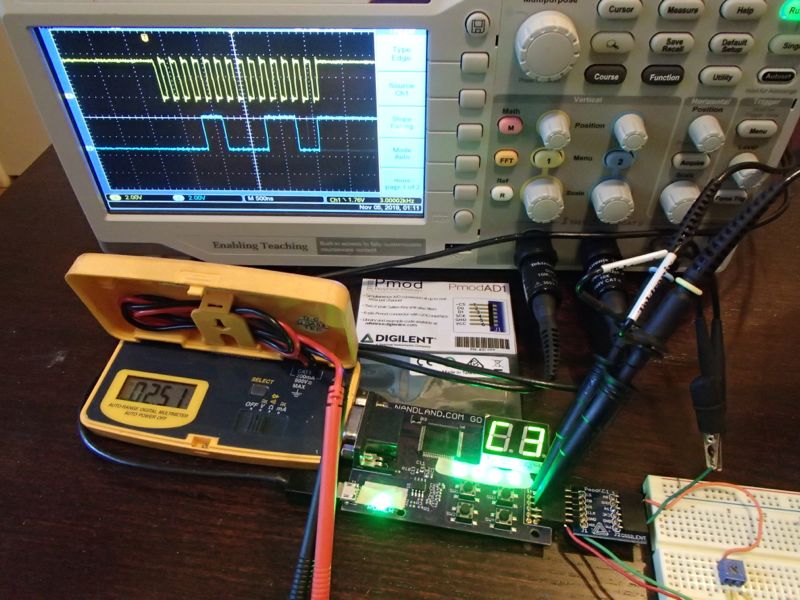
Here is a NanLand.com GoBoard with an FPGA running Verilog code (see below) that reads out a Digilent PmodAD1 ADC and shows the voltage using the LED displays.
The GoBoard’s FPGA is a Lattice HX1K, and the ADC board has two Analog Devices AD7476A 12 bit ADCs. Right now, the readout is 200 samples/s but in principle each ADC can do 1 million samples/s. My eventual goal is to make a 1 Ms/s two-channel oscilloscope.
Please see the video on YouTube: How to read an ADC with an FPGA
In you have questions about this setup, please contact me, either through this web page or by email at pghalverson “at” gmail “dot” com.
Also, be sure to visit the NandLand web site for fun tutorials. Without those tutorials I would be very frustrated!
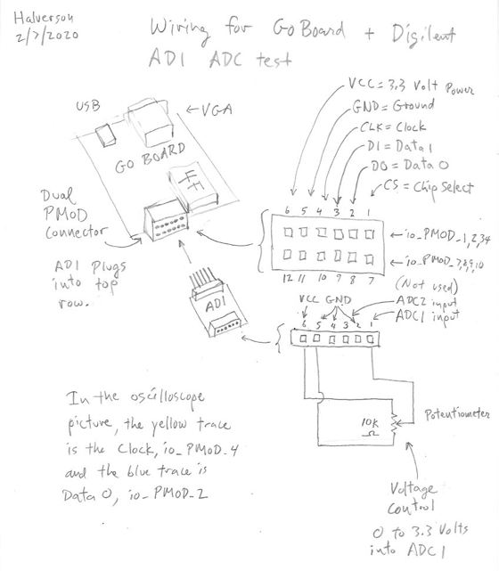
Connection diagram:
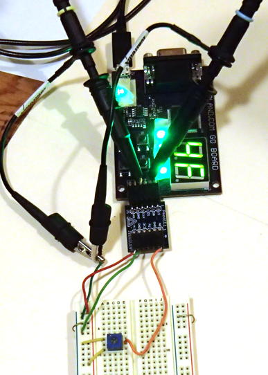
Connections photo:
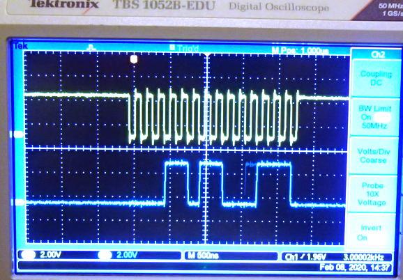
Scope signals:
====================================================================
Separate this Verilog code into three files to compile
// Filename: Read_ADC_Top.v
// Written by me, Peter Halverson, and posted on my web page http://halverscience.net/ Nov 4, 2019
// This Verilog code is intended to run on a GoBoard, available from nandland.com,
// and it uses a PmodAD1 analog-to-digital converter, available from Digilent
// This is the top module. NOTE: I had trouble with the Lattice LSE Synthesis tool
// not "autoguessing" that this is the top module. I had to explicitly tell the tool.
// To do that, go into Tool > Tool Options > LSE (tab) > Top Level Unit and type in "Read_ADC_Top"
module Read_ADC_Top
(input i_Clk, // Wire from the Main Clock, 25 MHz
output o_Segment1_A, // Wiring to the 1st 7-segment display.
output o_Segment1_B,
output o_Segment1_C,
output o_Segment1_D,
output o_Segment1_E,
output o_Segment1_F,
output o_Segment1_G,
output o_Segment2_A, // Wiring to the 2nd 7-segment display.
output o_Segment2_B,
output o_Segment2_C,
output o_Segment2_D,
output o_Segment2_E,
output o_Segment2_F,
output o_Segment2_G,
output o_LED_1, // Wiring to the LEDs
output o_LED_2,
output o_LED_3,
output o_LED_4,
output io_PMOD_1, // Wiring to the ADC board ~ chip select (active low)
input io_PMOD_2, // data from ADC 0
input io_PMOD_3, // data from ADC 1 (not used)
output io_PMOD_4, // clock to read out data
input i_Switch_1, // Wires to the switches. Not used now, but useful for debugging.
input i_Switch_2,
input i_Switch_3,
input i_Switch_4);
wire w_Segment1_A, w_Segment2_A;
wire w_Segment1_B, w_Segment2_B;
wire w_Segment1_C, w_Segment2_C;
wire w_Segment1_D, w_Segment2_D;
wire w_Segment1_E, w_Segment2_E;
wire w_Segment1_F, w_Segment2_F;
wire w_Segment1_G, w_Segment2_G;
wire w_LED_1, w_LED_2, w_LED_3, w_LED_4;
wire [11:0] w_ADC_Data;
wire w_ADC_Data_Valid;
reg [31:0] r_Readout_Count = 0;
parameter Readout_Period = 125000; // 125000 gives 200 per second (25 MHz clock / 125000 )
reg [11:0] r_ADC_Data; // Only low order 12 bits are used. Four high order bits always zero
reg r_ADC_Data_Requested = 1'b0;
// Code to read the ADC and put the results on the 7-segment display (upper 8 bits)
// and the LEDS (lower 4 bits)
always @(posedge i_Clk) begin
if (r_Readout_Count >= Readout_Period) begin
r_Readout_Count <= 0;
r_ADC_Data_Requested <= 1'b1; // Tell Read_ADC we want data
end else begin
r_Readout_Count <= r_Readout_Count + 1;
r_ADC_Data_Requested <= 1'b0;
end
if (w_ADC_Data_Valid == 1'b1) begin
//if (1'b1 == 1'b1) begin
r_ADC_Data <= w_ADC_Data; // Get the data from Read_ADC
end
end
// Interface (instantiation) to the code that triggers the ADC and reads its data.
// parameter ADC_CLKS_PER_BIT determines the readout speed of the bits from the ADC.
// Its the GoBoard's clock frequency divided by the parameter.
// Example: 25,000,000 / 25 would give 1 mega-baud.
// Maximum, according to Analog Devices AD7476 data sheet is 20 mega-baud
Read_ADC #(.ADC_CLKS_PER_BIT(4)) Read_ADC_Inst // 4 is gets me 6.25 Mbaud, 160 ns clock
(.i_Clock(i_Clk),
.i_ADC_Data_Serial(io_PMOD_2),
.i_ADC_Data_Requested(r_ADC_Data_Requested),
.o_ADC_Data_Valid(w_ADC_Data_Valid),
.o_ADC_Data(w_ADC_Data),
.o_ADC_Chip_Select_Not(io_PMOD_1),
.o_ADC_Clock(io_PMOD_4));
// Binary to 7-Segment Converter for Upper Digit, highest nibble of ADC data
Binary_To_7Segment SevenSeg1_Inst
(.i_Clk(i_Clk),
.i_Binary_Num(r_ADC_Data[11:8]),
.o_Segment_A(w_Segment1_A),
.o_Segment_B(w_Segment1_B),
.o_Segment_C(w_Segment1_C),
.o_Segment_D(w_Segment1_D),
.o_Segment_E(w_Segment1_E),
.o_Segment_F(w_Segment1_F),
.o_Segment_G(w_Segment1_G));
assign o_Segment1_A = ~w_Segment1_A;
assign o_Segment1_B = ~w_Segment1_B;
assign o_Segment1_C = ~w_Segment1_C;
assign o_Segment1_D = ~w_Segment1_D;
assign o_Segment1_E = ~w_Segment1_E;
assign o_Segment1_F = ~w_Segment1_F;
assign o_Segment1_G = ~w_Segment1_G;
// Binary to 7-Segment Converter for Lower Digit, middle nibble of ADC data
Binary_To_7Segment SevenSeg2_Inst
(.i_Clk(i_Clk),
.i_Binary_Num(r_ADC_Data[7:4]),
.o_Segment_A(w_Segment2_A),
.o_Segment_B(w_Segment2_B),
.o_Segment_C(w_Segment2_C),
.o_Segment_D(w_Segment2_D),
.o_Segment_E(w_Segment2_E),
.o_Segment_F(w_Segment2_F),
.o_Segment_G(w_Segment2_G));
assign o_Segment2_A = ~w_Segment2_A;
assign o_Segment2_B = ~w_Segment2_B;
assign o_Segment2_C = ~w_Segment2_C;
assign o_Segment2_D = ~w_Segment2_D;
assign o_Segment2_E = ~w_Segment2_E;
assign o_Segment2_F = ~w_Segment2_F;
assign o_Segment2_G = ~w_Segment2_G;
assign o_LED_1 = r_ADC_Data[3]; // Lowest nibble of ADC data will be displayed on the four LEDs
assign o_LED_2 = r_ADC_Data[2];
assign o_LED_3 = r_ADC_Data[1];
//assign o_LED_3 = i_Switch_3;
//assign o_LED_4 = i_Switch_4;
//assign o_LED_4 = r_Readout_Count[22];
assign o_LED_4 = r_ADC_Data[0];
endmodule // Read_ADC_Top
========================================================
// Filename: Read_ADC.v
// ADC Readout for Digilent PMOD AD1, which has two Analog Devices AD7476A 12-bit ADCs
// Written by Peter Halverson and posted on http://halverscience.net/ Nov. 4, 2019
// Based on UART RX from http://www.nandland.com
module Read_ADC
#(parameter ADC_CLKS_PER_BIT = 25)
(
input i_Clock,
input i_ADC_Data_Serial,
input i_ADC_Data_Requested,// Set this to True when you want an ADC readout
output o_ADC_Data_Valid, // When this is true, it means the adc data is ready
output [11:0] o_ADC_Data, //Its a 12 bit ADC
output o_ADC_Chip_Select_Not, // The ~CS line is active when False
output o_ADC_Clock // Falling edge requests next bit, bit is read on rising edge
);
parameter IDLE = 2'b00; // State Machine states
parameter ADC_CONVERSION_DELAY = 2'b01; // Not needed? Datasheet says 10 ns minimum is needed.
parameter READ_DATA_BITS = 2'b10;
parameter CLEANUP = 2'b11;
reg [7:0] r_Clock_Count = 0;
reg [3:0] r_Bit_Index = 15; //4 zero bits + 12 data bits = 16 bits total
reg [15:0] r_ADC_Data = 0; // First 4 bits always zero
reg r_ADC_Data_Valid = 0;
reg [2:0] r_SM_Main = 0;
reg r_ADC_Chip_Select_Not = 1;
reg r_ADC_Clock = 1;
reg [7:0] r_Delay_Clock_Count = 0;
reg r_Got_The_Bit = 1'b0;
// Read ADC state machine
always @(posedge i_Clock)
begin
case (r_SM_Main)
IDLE : begin
r_ADC_Data_Valid <= 1'b0;
r_Clock_Count <= 0;
r_Delay_Clock_Count <= 0;
r_Bit_Index <= 14; // ADC send 15 bits (not 16) High order bits first
r_ADC_Clock <= 1'b1;
if (i_ADC_Data_Requested == 1'b1) begin
r_SM_Main <= ADC_CONVERSION_DELAY;
r_ADC_Chip_Select_Not <= 1'b0; // Start the conversion
end else begin
r_SM_Main <= IDLE;
r_ADC_Chip_Select_Not <= 1'b1; // Don't start the conversion
end
end // case: IDLE
ADC_CONVERSION_DELAY : begin
if (r_Delay_Clock_Count < 0) begin // Adjust to give time for ADC to start a conversion
// 0 gives 80 ns (Three cycles of 25 MHz clock), 1 gives 120 ns, 2 gives 160 ns, etc
r_Delay_Clock_Count <= r_Delay_Clock_Count + 1;
r_SM_Main <= ADC_CONVERSION_DELAY;
end else begin
r_Delay_Clock_Count <= 0;
r_SM_Main <= READ_DATA_BITS;
end
end // case: ADC_CONVERSION_DELAY
READ_DATA_BITS : begin
if (r_Clock_Count < ADC_CLKS_PER_BIT-1) begin
if (r_Clock_Count < (ADC_CLKS_PER_BIT/2)) begin
r_ADC_Clock <= 1'b0; // Falling edge tells ADC to output a bit
r_Got_The_Bit <= 1'b0;
end else begin
r_ADC_Clock <= 1'b1; // Rising edge is when we get the bit. (It is now stable)
if (r_Got_The_Bit == 1'b0) begin
r_ADC_Data[r_Bit_Index] <= i_ADC_Data_Serial; // GET THE DATA BIT!!
r_Got_The_Bit <= 1'b1; //We want to latch the bit only once
// Check if we have received all bits
if (r_Bit_Index > 0) begin // We need to get more bits (We get 16 bits, 1st four are zero)
r_Bit_Index <= r_Bit_Index - 1; //ADC send bit 15 first, then bit 14, ...
r_SM_Main <= READ_DATA_BITS;
end else begin
r_ADC_Data_Valid <= 1'b1; // All 15 bits are now valid. Tell caller to get the data.
r_ADC_Chip_Select_Not <= 1'b1; // Stop the conversion
r_SM_Main <= CLEANUP;
end
end
end
r_Clock_Count <= r_Clock_Count + 1;
end else begin
r_Clock_Count <= 0;
end
end // case: READ_DATA_BITS
CLEANUP : begin // Stay here 1 clock
// r_Delay_Clock_Count <= 0;
r_SM_Main <= IDLE;
r_ADC_Data_Valid <= 1'b0;
end // case: CLEANUP
default :
r_SM_Main <= IDLE;
endcase
end
assign o_ADC_Data_Valid = r_ADC_Data_Valid;
assign o_ADC_Data = r_ADC_Data[11:0];
assign o_ADC_Chip_Select_Not = r_ADC_Chip_Select_Not;
assign o_ADC_Clock = r_ADC_Clock;
endmodule // Read_ADC
==============================================================
// Filename: Binary_To_7Segment.v
///////////////////////////////////////////////////////////////////////////////
// File downloaded from http://www.nandland.com
///////////////////////////////////////////////////////////////////////////////
// This file converts an input binary number into an output which can get sent
// to a 7-Segment LED. 7-Segment LEDs have the ability to display all decimal
// numbers 0-9 as well as hex digits A, B, C, D, E and F. The input to this
// module is a 4-bit binary number. This module will properly drive the
// individual segments of a 7-Segment LED in order to display the digit.
// Hex encoding table can be viewed at:
// http://en.wikipedia.org/wiki/Seven-segment_display
///////////////////////////////////////////////////////////////////////////////
module Binary_To_7Segment
(
input i_Clk,
input [3:0] i_Binary_Num,
output o_Segment_A,
output o_Segment_B,
output o_Segment_C,
output o_Segment_D,
output o_Segment_E,
output o_Segment_F,
output o_Segment_G
);
reg [6:0] r_Hex_Encoding = 7'h00;
// Purpose: Creates a case statement for all possible input binary numbers.
// Drives r_Hex_Encoding appropriately for each input combination.
always @(posedge i_Clk)
begin
case (i_Binary_Num)
4'b0000 : r_Hex_Encoding <= 7'h7E;
4'b0001 : r_Hex_Encoding <= 7'h30;
4'b0010 : r_Hex_Encoding <= 7'h6D;
4'b0011 : r_Hex_Encoding <= 7'h79;
4'b0100 : r_Hex_Encoding <= 7'h33;
4'b0101 : r_Hex_Encoding <= 7'h5B;
4'b0110 : r_Hex_Encoding <= 7'h5F;
4'b0111 : r_Hex_Encoding <= 7'h70;
4'b1000 : r_Hex_Encoding <= 7'h7F;
4'b1001 : r_Hex_Encoding <= 7'h7B;
4'b1010 : r_Hex_Encoding <= 7'h77;
4'b1011 : r_Hex_Encoding <= 7'h1F;
4'b1100 : r_Hex_Encoding <= 7'h4E;
4'b1101 : r_Hex_Encoding <= 7'h3D;
4'b1110 : r_Hex_Encoding <= 7'h4F;
4'b1111 : r_Hex_Encoding <= 7'h47;
endcase
end // always @ (posedge i_Clk)
// r_Hex_Encoding[7] is unused
assign o_Segment_A = r_Hex_Encoding[6];
assign o_Segment_B = r_Hex_Encoding[5];
assign o_Segment_C = r_Hex_Encoding[4];
assign o_Segment_D = r_Hex_Encoding[3];
assign o_Segment_E = r_Hex_Encoding[2];
assign o_Segment_F = r_Hex_Encoding[1];
assign o_Segment_G = r_Hex_Encoding[0];
endmodule // Binary_To_7Segment